Microelectronics and Nanoelectronics Devices and Systems


Microelectronics and Nanoelectronics Devices and Systems
Development of new techniques, processes, and architectures for nanoelectronics:
- Exploration into novel materials: ferroelectrics, resistive switches, oxide thin-films/semiconductors , phase transition materials, III-Vs, III-Nitrides, 2D materials, carbon nanotubes, and spintronics
- Devices: Thin-film transistors, Ferroelectrics FETs, Resistive RAM, FinFETs, Nanosheets
- Applications: computation, new computing architectures, neuromorphic/artificial intelligence, beyond-CMOS, displays, AR/VR, quantum
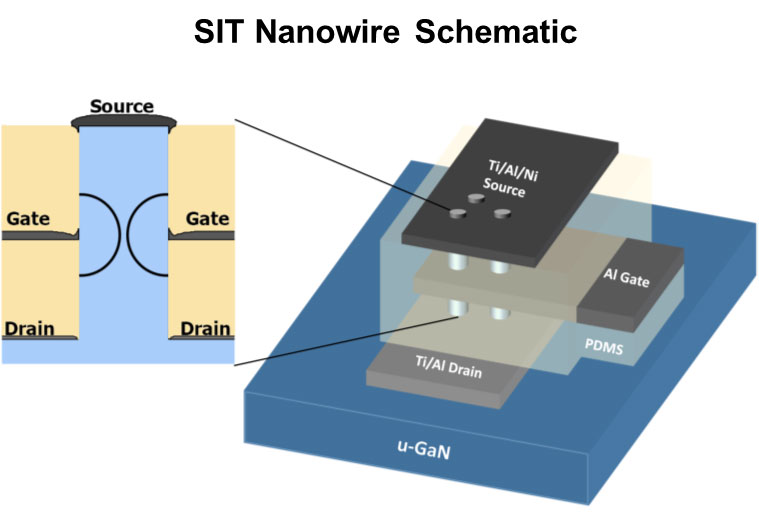
Vertical GaN Nanowire Static Induction Transistor (SIT)
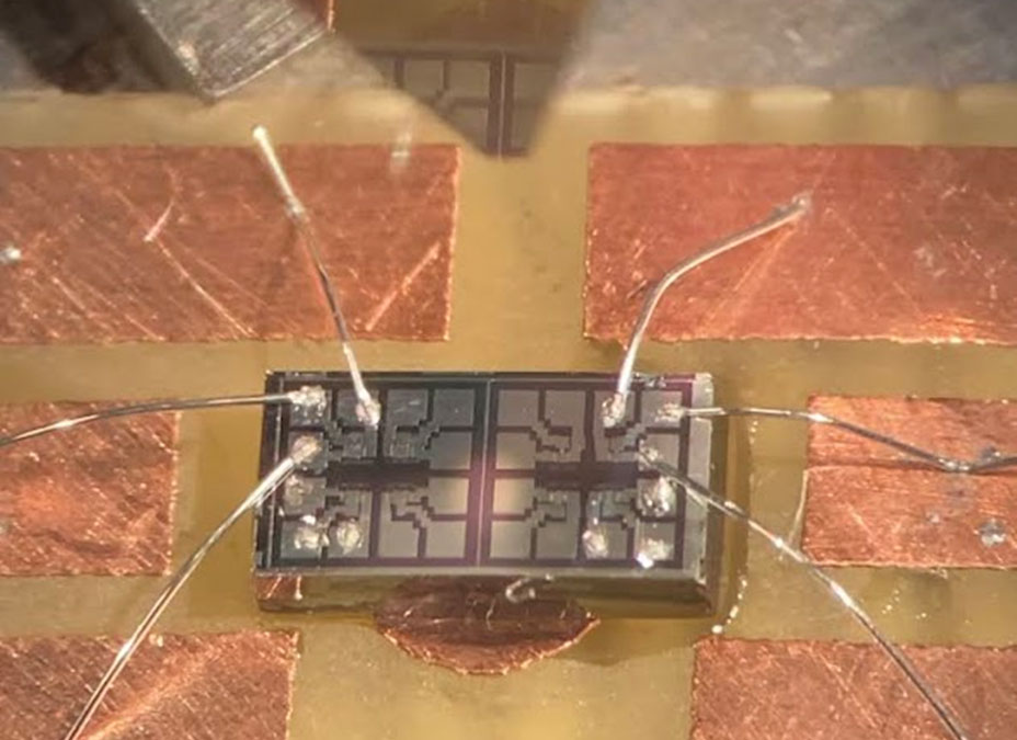
Wire-bonded metal gate PMOS transistors
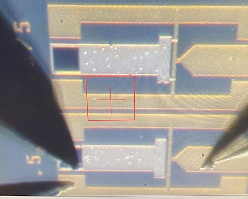
Electrical probe test of a 0.5-micron 2D graphene transistor

PMOS IC test chip designed and fabricated as a part of the semiconductor fabrication class. The students were trained on fabrication unit processes such as oxide growth, ion implantation and metal deposition, and the test structures consist of p-type FETs, resistors and logic gates.

Electric double layer gated 2D Field Effect Transistors based on epitaxially grown bi-graphene on a SiC substrate by Professor Ke Xu’s group. The chip includes side-gated FETs and side gated Hall bar devices with channel length ranging from 1 to 8 um.