The fine lines
A. Sue Weisler
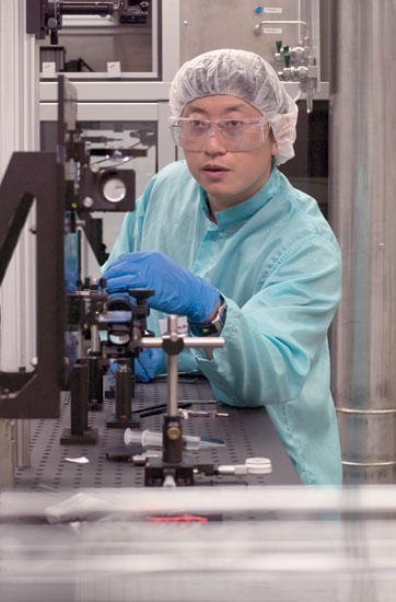
Researcher Jianming Zhou aligns the immersion lithographic system.
A wide variety of microchips – A.K.A. computer chips, integrated circuits or silicon chips – are produced to fulfill numerous different functions. Introduced in 1958, microchips have grown increasingly complex and powerful, while becoming smaller and less expensive. Today, for instance, a single computer microprocessor – just one type of chip – can pack more than 400 million transistors on a piece of silicon about the size of a thumbnail.
Chips are the basis of the modern electronics industry, essential for products ranging from cell phones and digital cameras to computers and iPods. Worldwide sales of chips totaled more than $200 billion last year.
The process of manufacturing these chips begins with an electronic circuit designed for a specific function. The circuit – which may contain millions of components on multiple layers – is converted into a pattern called a photomask. The microscopic masks function somewhat like a photographic negative; light is passed through the masks and the pattern is focused on a silicon wafer that has been coated with a light-sensitive material called a photoresist. The pattern becomes the guide for deposit of metal and silicon that will “grow” into the components of the chip. The process of imprinting the pattern on the wafer is called microlithography or nanolithography. The semiconductor industry currently produces chips with individual structures as small as 65 nanometers – smaller than a virus and 1,000 times finer than a human hair. (A nanometer is a billionth of a meter, which is 39.34 inches).
Research is underway worldwide to produce new generations of devices with even smaller circuitry. RIT’s Center for Nanolithography Research in 2004 was able to produce images of 31 nanometer resolution using a prototype liquid immersion lithography technique. In liquid immersion lithography, water is placed between the lens and the wafer when the pattern is projected onto the wafer. The liquid immersion process has allowed for higher imaging resolution, resulting in significantly finer circuit lines than in conventional projection lithography. This technique is now being used by major chip manufacturers.
Earlier this year, RIT researchers announced success in imaging rendered to 26 nanometers, using a breakthrough method called evanescent wave lithography. This technique makes use of the “evanescent field,” a characteristic of optical propagation at very large angles, leading to resolution beyond conventional means.


