RIT, photonic company build quantum chip prototype to bridge quantum and traditional network bands
Phase II of new grant awarded realizes promise of entangled photons toward faster, more secure computing systems
Elizabeth Lamark
RIT engineering and science faculty are working to develop quantum chip prototypes and network technology.
Quantum computing just became more entangled.
Researchers from Rochester Institute of Technology and national photonic device company, AdvR Inc., built a quantum chip prototype that is bridging today’s traditional fiber optic networks with the future—quantum computing networks.
By better entangling, or integrating, the two types of communications technologies, quantum-based computers would be able to process data orders of magnitude faster than current computers and to move information across networks more securely.
With speed and security coupled with higher sensing power based on quantum mechanics, this technology platform could further hone important computing applications for drug development or imaging, said Stefan Preble, principal investigator for RIT’s project team.
Stefan Preble
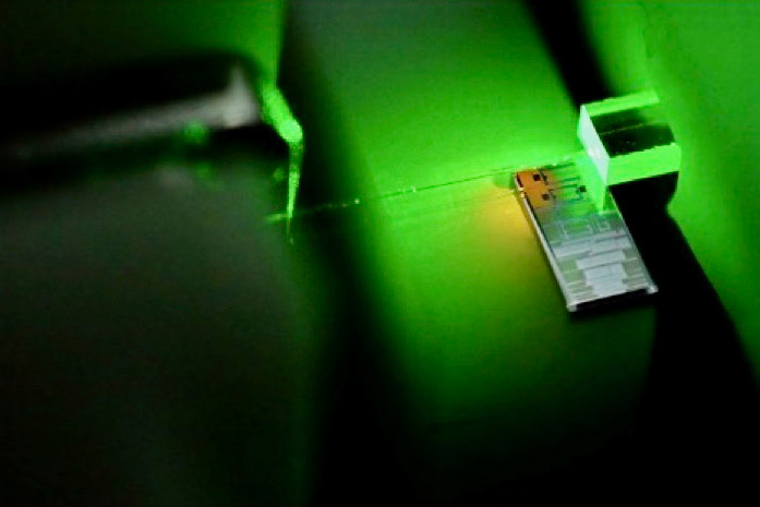
Faculty-researchers are integrating visible light photons in a KTP chip with silicon quantum photonic chips. This type of technology integration will enable a future quantum Internet
“Quantum has this promise for breakthroughs in many different disciplines, and this comes down to the fundamental level. Quantum behaviors are so different from the classical technologies that we have been designing,” said Preble, a professor of electrical and microelectronic engineering. He is also graduate program director of the university’s microsystems engineering doctoral program and a faculty-researcher with RIT’s Future Photon Initiative. With his extensive experience in developing photonic chips, Preble was part of the team that developed one of the first integrated quantum photonics wafers.
Building quantum technologies on chips continues to advance. The project, “AFRL STTR Phase II: Wideband quantum photonic integrated circuits for conditioning, routing and gate operations of highly non-degenerate entangled photons” is funded by a grant of nearly $700,000 from the Department of the Air Force Material Command, and is part of a larger initiative to realize quantum computers.
The basic technology concepts include operating over a wide range of wavelengths—both seen and unseen—to produce links between quantum nodes based on atomic, quantum systems and fiber optic infrastructure.
Some integrated photonic chips are being manufactured at semiconductor fabrication facilities. Most leverage silicon, which has long been the foundational material in chips. Production costs using the material are lower.
“But the problem with silicon is it doesn’t work at the visible wavelengths that we need for quantum nodes that utilize atoms. Silicon can’t solve everything,” said Preble. “With photons, their key advantage is they move at the speed of light, so they are really good at moving information, specifically quantum information, from place-to-place. That is our focus, to basically connect things together quantum-mechanically.”
Quantum technology is evolving, and a long-range goal is to develop an advanced Internet with quantum computers “talking” to each other. This involves the development of a bridge from atoms trapped in labs to optical fibers.
Greater distances, coupled with compatible technology along that route, can mean increased capability for quantum information and data. Also, use of varied materials and managing light sources for the integrated chips could improve the scalability of the production process. All these elements of the overall system are currently being researched and developed. Preble and co-PI Gregory Howland, assistant professor in RIT’s College of Science, are focusing on assessing a wider range of wavelengths, or colors, beyond the visible wavelengths.
“But the problem with that is the visible wave length photons don’t transmit efficiently over optical fibers,” said Preble, who has been developing integrated photonic chips for a decade, and this aspect of his work involves use of newer materials to integrate—or entangle—fiber optic capabilities with quantum-based technologies.
The project team found a solution in a quantum-compatible material with silicon photonic chips through research partner AdvR Inc., providing potassium titanyl phosphate, or KTP, for this hybrid integration. By taking the KTP-based chips and meshing them with silicon photonic chips, the team developed a hybrid, quantum photonic integrated circuit that is showing higher sensitivity and functionality than traditional chips.
AdvR Inc. develops optical components in several nonlinear optical material systems using KTP. It is well-suited to quantum advances because of several key qualities—waveguides, the devices that direct light—can be formed using traditional lithographic techniques allowing for arrayed outputs to match spacing and modal geometry of the silicon photonic integrated circuit input. KTP also has high resistance to optical damage, said Todd Hawthorne, a member of the project team and an optical engineer with AdvR, which is based in Bozeman, Mont.
“Perhaps mostly importantly for developing a useful optical quantum network, KTP, due to its particular dispersion properties can, for certain wavelengths and polarizations, produce high purity, spectrally un-entangled, photon pairs without significant spectral filtering,” Hawthorne said, adding that the next generation of high purity photons are needed for implementing advanced quantum networking protocols such as entanglement swapping to further develop a long-range quantum network. Further plans during this phase include integrating the KTP waveguide arrays with silicon photonic chips for post processing of the photon pairs.
The project extends through September 2022.


